Twist in the Tale: Exploring the Dielectric Screening Effect in Twisted Bilayer Graphene
© The Physical Society of Japan
This article is on
On Dielectric Screening in Twisted Double Bilayer Graphene
(JPSJ Editors' Choice)
J. Phys. Soc. Jpn.
90,
124702
(2021)
.
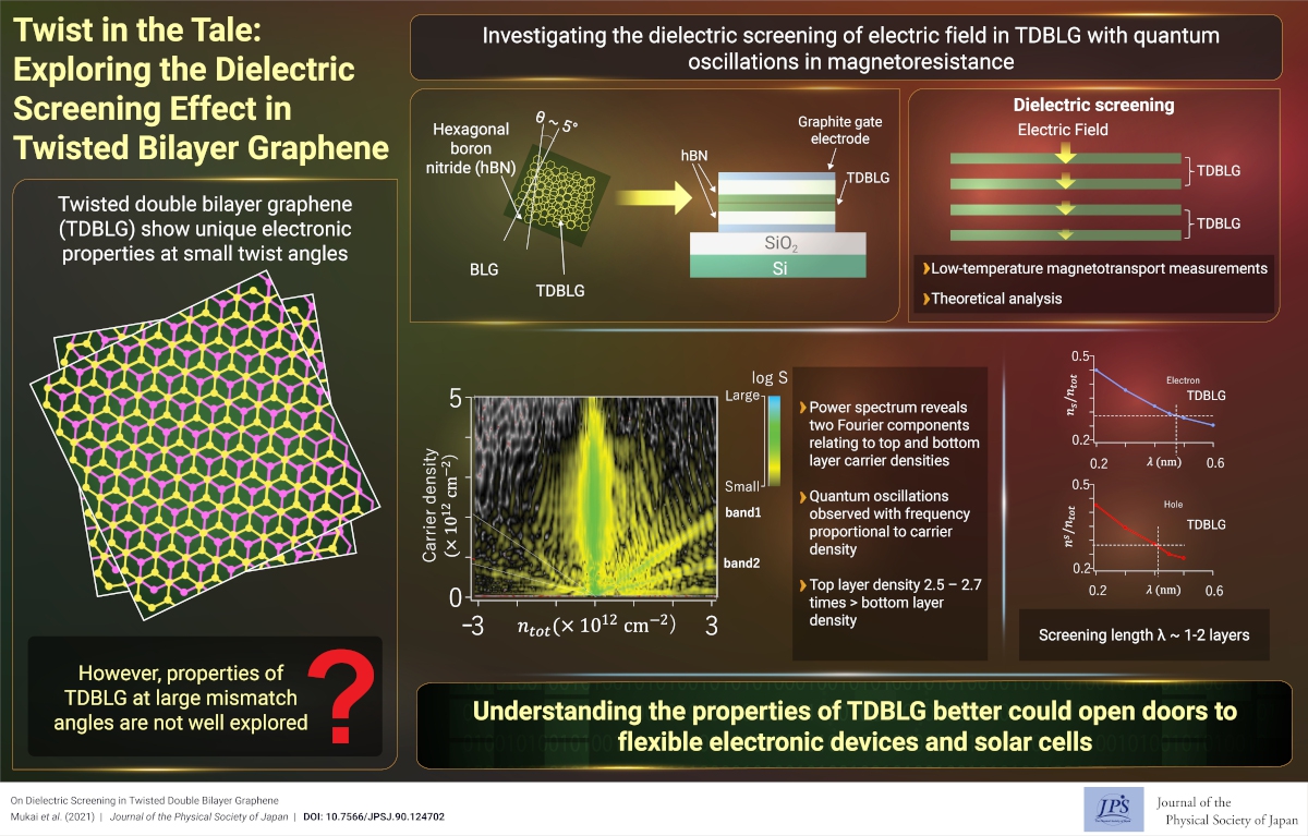
Although the screening of an external electric field, strongly influences the electronic states of two-dimensional material stack, it is not well understood. Magnetotransport measurements of twisted double bilayer graphene uncovered the screening of atomic layers.
It has been approximately a decade since Geim and Novoselov were honored with a Nobel prize for discovering graphene: a one-layer atomic sheet of graphite. Recently, a twisted stack of graphene (hereafter referred as twisted graphene) has been attracting an extensive attention. In its system, interesting phenomena are continuously being discovered, such as superconductivity and correlated insulating states. Twisted graphene has a characteristic feature: by stacking atomic layer graphene, a new ‘material’ can be produced without forming new chemical bonds. This differs from conventional materials.
A significant issue in designing the electronic band structure of a twisted graphene system and other stacked two-dimensional materials is the dielectric screening of an electric field applied via a gate voltage. Generally, when an electric field is applied to a conductor, electrons travel in the conductor so that no electric field is present inside it; as a result, the surface of the conductor become charged. This is known as electrostatic screening. However, what happens if the conductor is composed of a few layers of atomically thin graphene? Will only the surface layer be charged, or will all layers be charged uniformly? Discussions on this issue can be traced back to historic studies on graphite and its intercalation compounds. Indeed, this type of screening is important when designing or analyzing the electronic band structure at the device in operation.
The study explores this issue by conducting a low temperature transport experiment using twisted double bilayer graphene, which is a stack of bilayer graphene sheets whose relative crystal angle is adjusted by approximately 5°; this is considerably larger than the magic angle. The bilayer graphene was prepared by using the Scotch-tape-method.
Measurements at low temperatures and in a magnetic field exhibited quantum oscillations, which reflect the carrier density of the electronic band. Two bands with different carrier densities were revealed, which reflect the screened electric field of the gate voltage. The screening length was slightly longer than that of AB-stacked four-layer graphene, a material that has the same number of layers, but a stacking structure is the same as a natural graphite crystal. The results may correspond to the difference in the features of quantum mechanical wave functions perpendicular to the plane.
The present knowledge and methods could be used to tailor the valley structure of the band structure of the twisted graphene systems. We expect that solar cells or novel transistor devices based on new principles, will be realized in the near future. Diamonds are the queen of jewelry. Carbon fibers are a key item in sports. Therefore, will carbon also revolutionize electronics?
(Written by R. Yagi on behalf of all authors)
On Dielectric Screening in Twisted Double Bilayer Graphene
(JPSJ Editors' Choice)
J. Phys. Soc. Jpn.
90,
124702
(2021)
.
Share this topic


Fields
Related Articles
-
Enhancing Accuracy and Reliability Bayesian Framework for Analysis of AR-HAXPES of Hard X-ray Photoelectron Spectroscopy
Dielectric, optical, and other properties in condensed matter
Electronic structure and electrical properties of surfaces and nanostructures
Measurement, instrumentation, and techniques
2026-4-28
We present a Bayesian framework for angle-resolved hard X-ray photoelectron spectroscopy (AR-HAXPES), combining Replica Exchange Monte Carlo with hierarchical integration to objectively and precisely estimate thin-film thickness.
-
What Shapes Electron Distributions in Nonequilibrium Nanowires?
Electronic transport in condensed matter
2026-4-20
A theoretical framework was developed to describe nonequilibrium electron distributions across the ballistic, diffusive, and local equilibrium transport regimes in voltage-biased nanowires in a unified manner.
-
Toward Clarification of Physical Properties of Quasicrystals: Noncollinear Magnetic Orders in Icosahedral Approximants
Cross-disciplinary physics and related areas of science and technology
Electronic transport in condensed matter
Magnetic properties in condensed matter
2026-4-6
An effective model based on magnetic anisotropy arising from a crystalline electric field is constructed for icosahedral approximants, which not only explains measured ferromagnets and antiferromagnets but also reveals new types of noncollinear magnetic orders.
-
Definitive Momentum and Spin Imaging Resolves 20-Year Debate on Gold Surface Spin
Electronic structure and electrical properties of surfaces and nanostructures
Magnetic properties in condensed matter
2026-4-1
Researchers at the Institute for Molecular Science (IMS) have utilized a cutting-edge Photoelectron Momentum Microscope (PMM) at the UVSOR Synchrotron Facility to settle a two-decade-long controversy concerning the direction of electron spin on the Au(111) surface. This study provides a definitive, full-map, comprehensive reference for quantum imaging that is essential for advancing spintronics technology.
-
Oxide Superionic Conductivity of a-Axis-Oriented Ce0.75Sm0.25O2−δ Thin Film
Electronic structure and electrical properties of surfaces and nanostructures
2026-2-2
Highly a-axis oriented Ce0.75Sm0.25O2-δ thin film fabricated on a yttria-stabilized zirconia substrate achieved oxide superionic conductivity, which can apply as an electrolyte in solid oxide fuel cells operating at medium temperature.