How to Construct a 3D Dirac Semimetal by Stacking 2D Massless Dirac Fermion Layers
© The Physical Society of Japan
This article is on
Three-Dimensional Topological Semimetal/Insulator States in α-Type Organic Conductors with Interlayer Spin-Orbit Interaction
J. Phys. Soc. Jpn.
93,
123703
(2024)
.
Interlayer spin–orbit coupling originating from the anion potential gives rise to a 3D Dirac semimetal state that preserves inversion symmetry in the multilayer organic massless Dirac fermion system α-(ET)2I3.
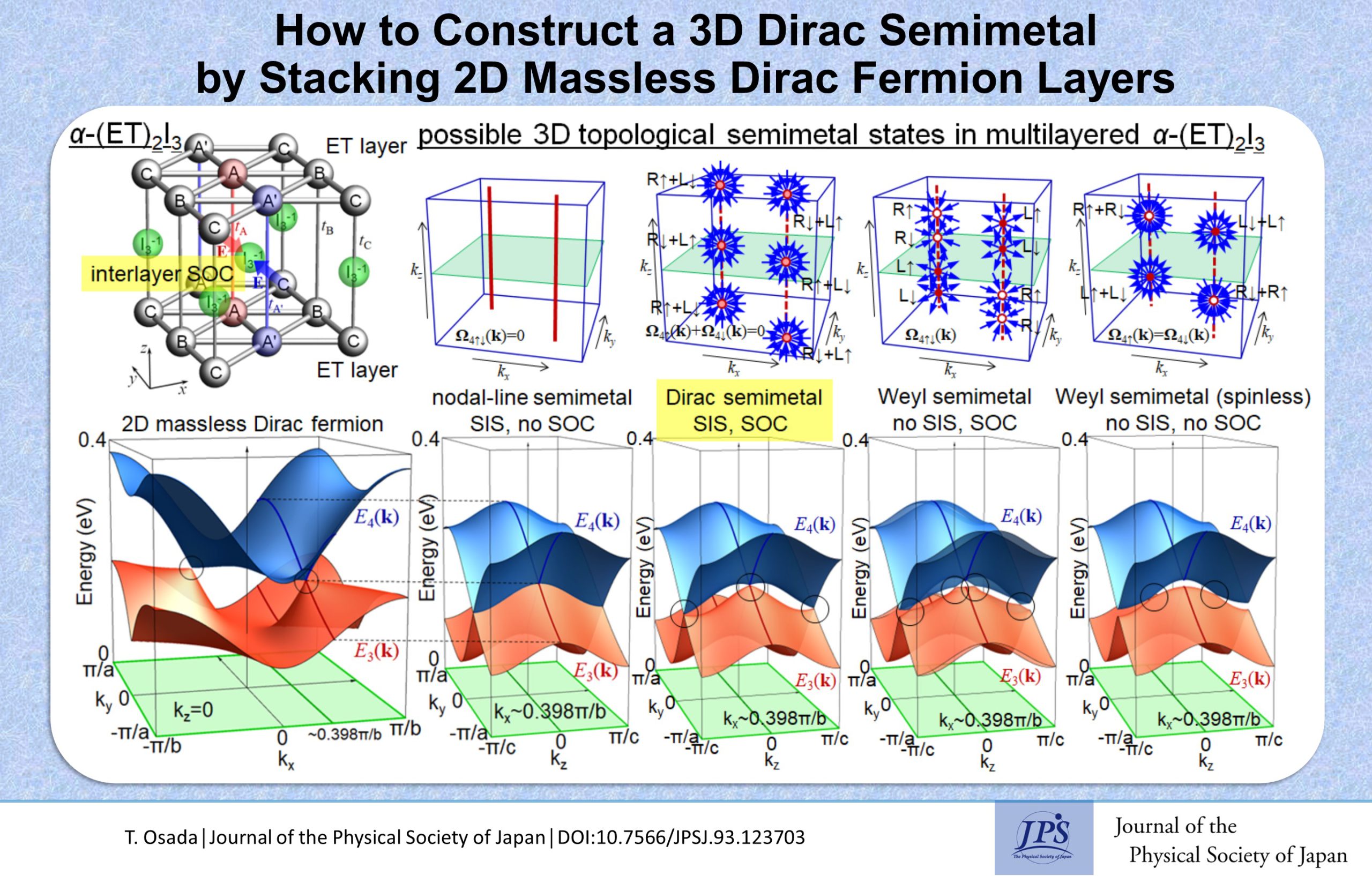
Dirac and Weyl semimetals are three-dimensional (3D) topological semimetals in which the conduction and valence bands touch at nodal points with a linear dispersion in the 3D Brillouin zone (BZ). They exhibit characteristic magnetotransport phenomena, negative longitudinal magnetoresistance and a planar Hall effect, resulting from the chiral anomaly. Recently, a layered organic conductor, α-(ET)2I3, exhibited these phenomena at low temperatures, indicating that it is a 3D Dirac or Weyl semimetal. However, it is well established that each ET layer of α-(ET)2I3 is a two-dimensional (2D) massless Dirac fermion system, where the conduction and valence bands touch at two nodes in the 2D BZ. Therefore, the question is whether and how 3D Dirac or Weyl semimetals can be formed by stacking 2D massless Dirac fermion layers.
Because the α-(ET)2I3 crystal has space inversion symmetry (SIS) and time reversal symmetry (TRS), the stacking must preserve these symmetries. Under SIS and TRS, the Weyl semimetal is never allowed, but the Dirac semimetal can be allowed because the total Berry curvature of the spin-degenerate bands is cancelled out. However, when simple interlayer hopping is introduced into the electronic structure model without breaking the SIS and TRS, the system usually becomes a 3D nodal-line semimetal, where 2D nodal points form nodal lines along the stacking direction in the 3D BZ. To realize a Dirac semimetal, we must consider spin–orbit coupling (SOC) in interlayer hopping. In the α-(ET)2I3 crystal, the ET conduction layer and the I3− anion layer are alternately stacked. Electrons hopping from one ET layer to the neighboring ET layer must penetrate the I3− layer, and the I3− configuration is unsymmetrical around some hopping paths. In fact, the I3− ion is located on one side of the interlayer hopping path between the A (or A’) sites of the neighboring layers and imposes a strong potential gradient on the hopping electrons, resulting in SOC. Note that SOC is relatively strong in interlayer hopping; however, it is generally considered weak in the ET layers because the ET molecule consists of light atoms. This interlayer SOC reflecting the I3− configuration opens a gap along the nodal line in the interlayer kz-dispersion, leaving two Dirac points at kz = 0 and π/c. Therefore, the interlayer SOC arising from the anion potential can realize the Dirac semimetal state while maintaining the SIS and TRS. If the SIS is broken by the introduction of interlayer hopping, each band exhibits zero-field spin splitting, and the Weyl semimetal state, where spin degeneracy is lifted, arises instead of the Dirac semimetal state.
(Written by Toshihito Osada on behalf of the authors)
Three-Dimensional Topological Semimetal/Insulator States in α-Type Organic Conductors with Interlayer Spin-Orbit Interaction
J. Phys. Soc. Jpn.
93,
123703
(2024)
.
Share this topic


Fields
Related Articles
-
Enhancing Accuracy and Reliability Bayesian Framework for Analysis of AR-HAXPES of Hard X-ray Photoelectron Spectroscopy
Dielectric, optical, and other properties in condensed matter
Electronic structure and electrical properties of surfaces and nanostructures
Measurement, instrumentation, and techniques
2026-4-28
We present a Bayesian framework for angle-resolved hard X-ray photoelectron spectroscopy (AR-HAXPES), combining Replica Exchange Monte Carlo with hierarchical integration to objectively and precisely estimate thin-film thickness.
-
Definitive Momentum and Spin Imaging Resolves 20-Year Debate on Gold Surface Spin
Electronic structure and electrical properties of surfaces and nanostructures
Magnetic properties in condensed matter
2026-4-1
Researchers at the Institute for Molecular Science (IMS) have utilized a cutting-edge Photoelectron Momentum Microscope (PMM) at the UVSOR Synchrotron Facility to settle a two-decade-long controversy concerning the direction of electron spin on the Au(111) surface. This study provides a definitive, full-map, comprehensive reference for quantum imaging that is essential for advancing spintronics technology.
-
Oxide Superionic Conductivity of a-Axis-Oriented Ce0.75Sm0.25O2−δ Thin Film
Electronic structure and electrical properties of surfaces and nanostructures
2026-2-2
Highly a-axis oriented Ce0.75Sm0.25O2-δ thin film fabricated on a yttria-stabilized zirconia substrate achieved oxide superionic conductivity, which can apply as an electrolyte in solid oxide fuel cells operating at medium temperature.
-
Hybrid Quantum-Classical Computing for Quasiparticle Band Structures
Electron states in condensed matter
Mathematical methods, classical and quantum physics, relativity, gravitation, numerical simulation, computational modeling
2025-12-12
The proposed hybrid quantum-classical computing method enables practical calculations of quasiparticle band structures to expand the possibilities for quantum materials research.
-
Topological Photonics: Recent Advances in Controlling Light
Cross-disciplinary physics and related areas of science and technology
Dielectric, optical, and other properties in condensed matter
Electromagnetism, optics, acoustics, heat transfer, and classical and fluid mechanics
Electronic structure and electrical properties of surfaces and nanostructures
Structure and mechanical and thermal properties in condensed matter
2025-12-8
The special topics edition of the Journal of the Physical Society of Japan presents five new review articles offering cutting-edge information on the emerging field of topological photonics.