

Angle-Resolved Photoelectron Spectroscopy Microscopy: A Tool to Accelerate Nanomaterials Research
© The Physical Society of Japan
This article is on
Domain-Resolved Photoelectron Microscopy and µm-Scale Momentum-Resolved Photoelectron Spectroscopy of Graphite Armchair Edge Facet
(JPSJ Editors' Choice)
J. Phys. Soc. Jpn.
91,
094703
(2022)
.
Researchers have published a practical guide on new uses of photoelectron microscopy combined with valence band dispersion analysis. They visualized several-micrometers-wide graphite facets and precisely characterized the band structure.
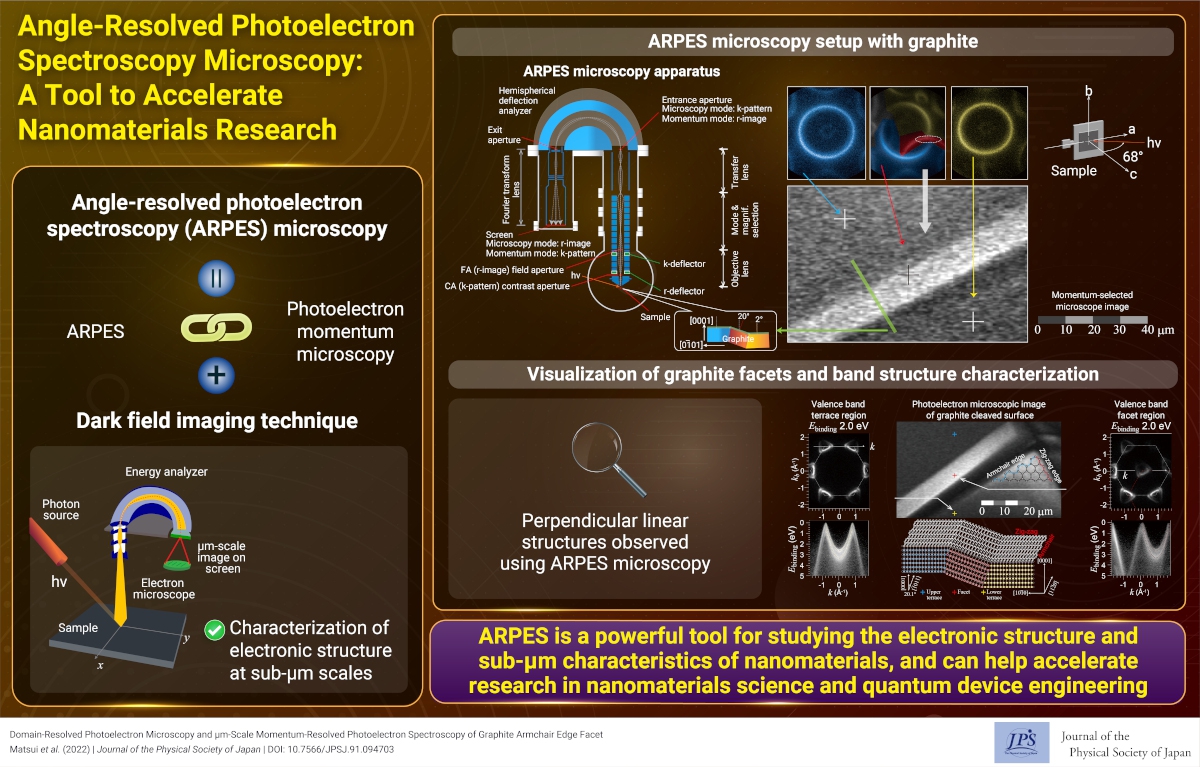
In recent years, the integration of high-resolution spectroscopy and microscopic imaging has attracted considerable attention owing to the demand in the fields of materials science and device engineering to elucidate the atomic structure and valence electron behavior for determining the material properties of sub-μm-scale polycrystalline composites and highly integrated structures. Angle-resolved photoelectron spectroscopy (ARPES) measures the angular distribution (momentum space distribution) of photoelectrons emitted from the sample surface irradiated with X-rays and reveals the composition and electronic structure of the sample. Photoelectron emission microscopy (PEEM) captures photoelectrons using a cathode lens and projects a magnified real-space image of the photon-irradiated region onto a two-dimensional detector. Photoelectron momentum microscopy (PMM) is a new type of PEEM that has greatly improved the projection range in the momentum space as well as the energy resolution and facilitates ARPES measurements in minute areas. In low-energy electron microscopy (LEEM) that uses electrons as the excitation source, a technique called dark-field imaging has been developed to select electron diffraction spots in momentum space and visualize the spatial distribution of specific domains. Recently, researchers at the UVSOR Synchrotron Facility in Okazaki have applied the LEEM dark-field imaging method to PMM and established a momentum-selective photoelectron microscopy method; this is a new development in microscopic ARPES measurements.
Figure 1 shows an example of a local electronic structure measurement on a graphite cleaved surface by PMM. When a hexagonal single-crystal graphite flake is viewed with an optical microscope, many lines perpendicular to the edges are observed. From the shape of the valence band dispersion, the crystal orientation and interlayer distance in the local region can be identified. The π-dispersion of the valence band of graphite is the strongest at the M saddle point in the Brillouin zone. By selectively measuring the photoelectron intensity in the M direction of each region, a photoelectron microscopic image showing each region with a contrast with a resolution of about 100 nm can be projected. This technique reveals perpendicular linear structures as twinned graphite domains formed by folding. This report describes the momentum-selective photoelectron microscopy technique in detail.
This momentum-selective photoelectron microscopy technique has been applied in the visualization of monolayer step edges on the graphite surface and domain observation of thin film growth. Future applications are expected to meet the demands of microscopic spectroscopy research in nanomaterials science and quantum device engineering.
(written by Fumihiko Matsui on behalf of all authors.)
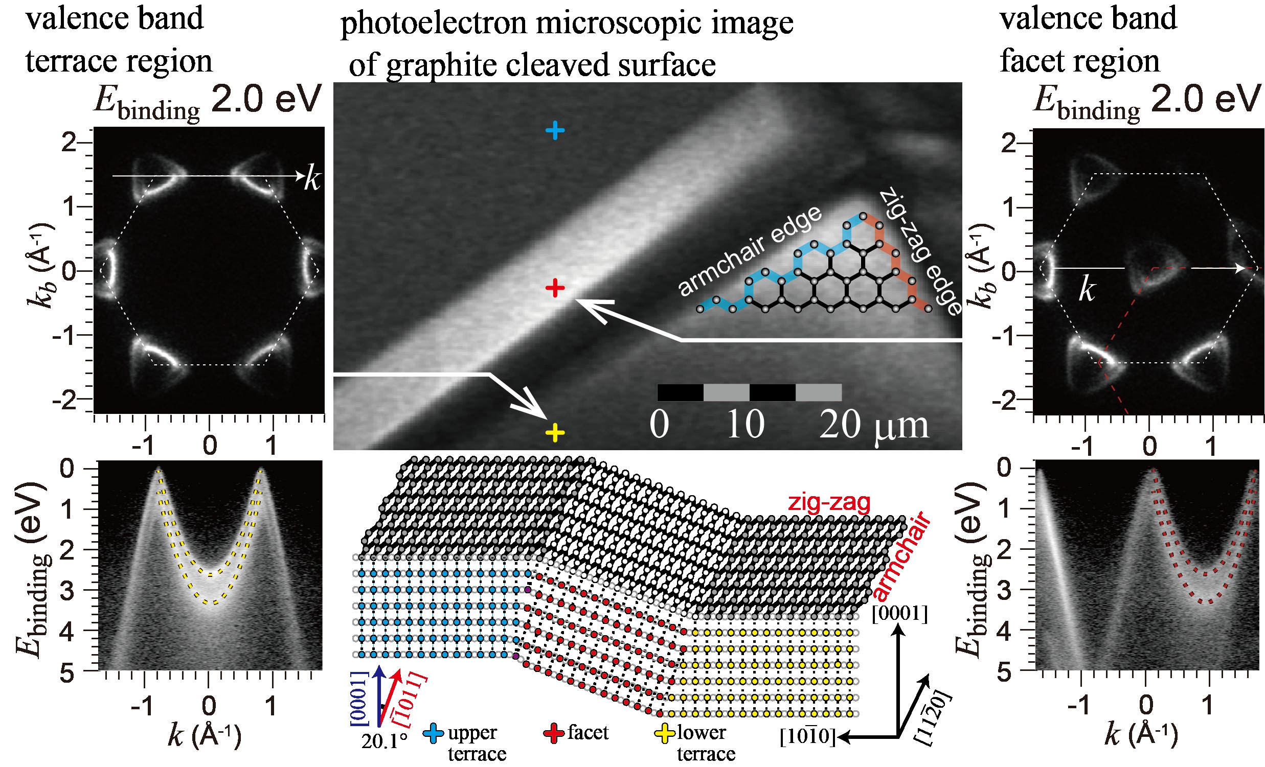
Figure 1: (Center) Domain-selected photoelectron microscopic image and the atomic structure model of the facet structure on the cleaved graphite surface. Valence photoelectron patterns and band dispersions from (left) terrace and (right) facet regions are shown together.
Domain-Resolved Photoelectron Microscopy and µm-Scale Momentum-Resolved Photoelectron Spectroscopy of Graphite Armchair Edge Facet
(JPSJ Editors' Choice)
J. Phys. Soc. Jpn.
91,
094703
(2022)
.
Share this topic


Fields
Related Articles
-
Topological Defects as Seeds of Phase Separation: Insights from a Minimal Lattice Model
Cross-disciplinary physics and related areas of science and technology
Statistical physics and thermodynamics
2026-7-13
A minimal lattice model revealed that topological defects with winding number +1 serve as nucleation sites for phase separation in active matter systems.
-
A Deep Dive Into AI-Driven Materials Science
Cross-disciplinary physics and related areas of science and technology
2026-7-6
This review from the Journal of the Physical Society of Japan examines how artificial intelligence overcomes traditional materials science bottlenecks, highlighting the shift from intuition-based discovery to data-driven innovation.
-
Peculiar Magnet Pointing Against an Applied Magnetic Field
Cross-disciplinary physics and related areas of science and technology
Magnetic properties in condensed matter
2026-7-1
TbNiC2 exhibits negative magnetization. A new mechanism, based on the coupling between the charge density wave and the antiferromagnetic order, is proposed to account for this peculiar phenomenon.
-
The Thermal Einstein–de Haas Effect: Theoretical Prediction and Observability in Chiral Carbon Nanotubes
Cross-disciplinary physics and related areas of science and technology
Structure and mechanical and thermal properties in condensed matter
2026-6-22
Although the Einstein–de Haas (EdH) effect describes material rotation in a magnetic field, a thermal EdH effect, driven by a temperature gradient, remains unobserved. Recently, chiral carbon nanotubes were theoretically proposed as promising candidates to observe it.
-
Negative Apparent Viscosity in Liquid Crystals
Cross-disciplinary physics and related areas of science and technology
Electromagnetism, optics, acoustics, heat transfer, and classical and fluid mechanics
Structure and mechanical and thermal properties in condensed matter
2026-6-8
Electrically driven liquid-crystal turbulence generates self-sustained flow and negative apparent viscosity. The fluorinated, chemically robust nematic PPDFB shows a substantially larger negative-viscosity effect than Schiff-base nematics.